
Download this article in PDF format.
Here atKeysight示波器总部,我们讨论了很多关于ASIC(应用程序特定的集成电路)。但为什么?谁在乎便宜的示波器的内部建筑?重要的是它的工作原理,对吗?我们同意。这就是为什么我们设计和使用自定义示波器特异性芯片的原因。
但是如何?这不像定制的ASIC只是出于稀薄的空气而出现。这需要多年的细心计划和研发工作。我们开发ASIC的原因有三个主要原因:性能,可靠性和成本。让我们快速了解性能方面,然后再看一下如何制作ASIC。
Performance
这通常是创建我们自己的ASIC的驱动动力。我们喜欢在可能的情况下使用现成的组件,但通常是不可能的。例如,我们的研究级Infiniium Z系列示波器的样品速率高达160 Gsamples/s。祝您好运找到现成的160个样本/S模数转换器(ADC)。即使您可以找到一个,它也可能无法满足示波器使用的严格噪声规格要求。因此,我们自己做到了。如果您发现自己处于类似情况,并且没有像我们一样拥有ASIC设计团队,那么大部分都可以与第三方签约。
Then, what happens once you have the world’s fastest ADC? How do you handle all of that data? An oscilloscope must save, plot, measure, and process that data in near real-time. You could offload it into a processor or FPGA (which we do for some things), but to get data analyzed the way we need at the speed we need, we opt for a digital ASIC.
ASIC的制作
创建ASIC涉及几个不同的步骤。在任何芯片开始开发之前,必须有一个长期的产品计划 - 设计师想在五到十年的时间里有什么?将来的产品将需要新功能或功能,有时需要ASIC(Fig. 1).
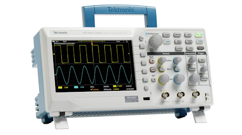
1. A custom 8-GHz oscilloscope ADC ASIC is used inKeysight’s S-Series Infiniium oscilloscopes.
Planning
First, there’s the planning team. They ask: “What chips do we need in a few years? Let’s make that.” And: “What can we get off-the-shelf in a few years? Let’snotmake that.” The planners also make performance vs. cost decisions (power consumption, transistor size, device speed, etc.).
Furthermore, an ASIC is typically classified as either digital or analog. Analog chips are basically signal-conditioning chips designed to manipulate signals into a more usable form. Digital chips are more or less streamlined FPGAs, designed for processing data inputs and providing usable data outputs (like an oscilloscope trace). There’s also athirdASIC的类型 - 像ADC一样的混合信号芯片(Fig. 2).
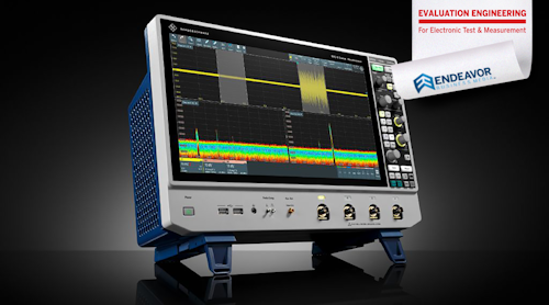
2.这些是Keysight-Custom ADC和Keysight上的处理器芯片cheap oscilloscope.
Digital ASICs
Let’s look a little closer at digital ASICs, like theKeysight来自Infiniiivision示波器的巨型示波器处理器。
前端/RTL设计
Once the chip is defined, the front-end team gets to work. They’re responsible for what’s known as “register-transfer-level” (RTL) design (and usually spend their time using Verilog or VHDL). Their job is to create a functional digital model of the chip—but not a physical model. The RTL team takes the chip’s functionality requirements and turns it into actual logic and computation models. To do this, they use digital design building blocks and modern digital logic techniques like adders, state machines, etc.
As the front-end team works, a test team is working to check the RTL for bugs. The goal is to try to avoid problems like the famous Pentium FDIV bug in 1995 that cost Intel nearly $500 million.
一旦测试团队验证RTL,它就会得到synthesizedinto aNetlist. This basically means that the RTL is turned from logic blocks into standard logic gates. Today, this is done by software, but historically engineers used truth tables and Karnaugh maps. This netlist is then put through a formal verification tool to ensure that it implements the functionality described by the RTL before being handed to the back-end team.
Back-end
Once the logic is verified, it’s time to physically lay out and implement the chip. This is known as “floorplanning.” Floorplanners use crazy-expensive software ($500k wouldn’t be unreasonable) to place the RTL design onto the chip footprint. In the real world, though, the front-end team passes early versions of the netlists to the back-end team so that they can get started on preliminary floorplanning work.
The back-end team starts with general placement of design blocks on the ASIC. The back-end team’s general workflow is:
- Floorplanning
- 位置
- 钟树建造
- 路由
- Optimization
- Static timing analysis
For the chip to work properly, gates involved in the same computations need to be physically close together. Also, designers make sure that power can be distributed efficiently throughout the chip. Power integrity is crucial for performance because it affects the speed of the gates’ operation. A gate getting a lower voltage than expected will operate more slowly than spec’d, and can cause unexpected timing errors.
Clock treesare added in at this point. A clock tree is a clock distribution network designed to make sure the clock reaches each gate at the right time. If clock edges showed up at different times to different parts of the chip, it would cause serious functional issues in the chip.
3.示波器采集板上的门之间的连接是自动连接的。
放置后,软件自动路由门之间的连接。您可能已经听到了“永远不要相信自动者”一词。但是,对于这种复杂性,这是唯一的选择,除非您想手动路由数十万(或数百万)连接(Fig. 3).
最后,整个过程中的关注点是该设计是否可以在物理上制造。可以使用设计规则检查(DRC)对此进行验证。基本上,这是一组参数设计师为该软件提供的,以说明哪些体系结构(物理形状)是而且不能用于制造。然后,该软件进行布局与原理检查(LVS),以确保物理几何形状创建所需的电路。
胶带
一旦前端和后端团队完成,the consensus is that it’s party time (and possibly nap time). This stage, called “tape out,” is when the final chip design is prepped for production. Massive files are sent to the fab, which then creates photomasks for each layer of the ASIC. It’s not uncommon for there to be 30-50 masks for a single chip.
Manufacturing
制作口罩后,使用一套不同的技术来制造芯片。当前的制造工艺需要将光刻,酸性浴,离子植入,炉子退火(烘烤)和金属溅射沉积结合使用。
然后,对制造的晶片进行了制造错误测试。根据晶圆的大小和过程复杂性,计划人员通常可以预测每个芯片的故障率。微小的异常,例如面具中的尘埃斑点,可能会导致故障。要检查故障,“扫描测试”用于检查每个单独的门。扫描测试是一套预定的信号套件,可测试芯片上的每个门。晶圆被锯入单独的模具,每个功能性模具都被传递给包装。
打包
工作模具被放入包裹并重新测试。包装团队通常会为模具设计自定义包装。包装团队必须考虑信号完整性,成本,热调节和设计的可靠性。通常,在Keysight,我们将更新当前使用的ASIC包装,以提高可靠性并降低示波器的硬件成本。
For example, the ADC on our low-cost oscilloscopes is the same ASIC used in some legacy oscilloscopes. However, by improving the packaging, we’ve reduced the packaging cost by nearly 5X. Thanks to that cost reduction, the ADC once used for a top-of-the-line oscilloscope can be used in our low-cost oscilloscope, the InfiniiVision 1000 X-Series.
Support Circuitry
4. Shown is the custom packaging and support circuitry for an Infiniium oscilloscope.
Finally, once a chip is manufactured, tested, and packaged, it still needs support circuitry(图4). For example, an op amp isn’t very useful if you never configure it with resistors! In the case of an oscilloscope, the ADC and processor chip must have appropriate signal-conditioning hardware on the acquisition board to make the signals usable by the chips.
这个怎么做的
So, while you shouldn’t use this article to go make your own ASIC, you should have a good idea of the process. It’s certainly a lot of work and planning, but the benefits of custom integrated circuits over FPGAs often make the investment worth it. For any given HP/Agilent/Keysightoscilloscope, several different ASICs are employed. We use analog ICs for a scope front end, a custom low-noise ADC for signal acquisition, and a custom processor to handle the digitized data. While the non-recoverable engineering expense (NRE) can be large, using the same chip in our $45,000 oscilloscopes and our $450 oscilloscopes earns the scopes a special place on the budget-conscious engineer’s bench.