.")
由于台湾台湾半导体制造公司和三星介绍了基于7纳米米制造芯片的能力,英特尔的制造业领导人在过去的一年中消失了。英特尔(Intel)的10纳米流程落后了,这使诸如高通和AMD之类的竞争对手将生产外包给了一个千载难逢的机会,可以放松其对个人计算机和数据中心市场的持有。
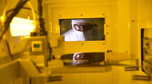
But Intel is attempting to retake the lead with smarter—not smaller—manufacturing. The Silicon Valley company said it has started stacking computer chips in three dimensions and bonding them together in an attempt to simplify the development of custom chips. The 3D stacking technology, Foveros, gives Intel the ability not only to improve energy efficiency and speed but also respond faster to customer demands.
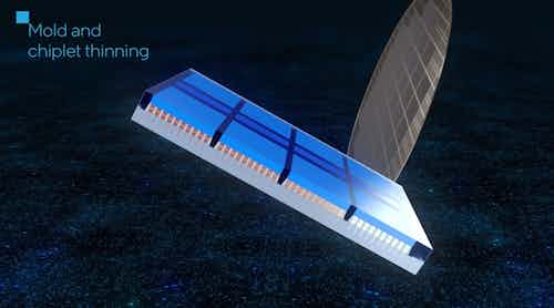
这家耗资620亿美元的公司成立于五十年前,他说,它将开始用较小的硅单元建造芯片,更常见于奇普莱特。每个设备都有一个特定的功能,并且使用高带宽互连使它们的作用似乎都在同一模具上。Foveros技术应允许英特尔在同一设备中提供新的内存和逻辑组合。
英特尔表示,没有其他公司可以extend die stacking to high-performance logic, including CPU, GPU and AI cores. Intel says the first product based on the Foveros architecture will be available the second half of 2019. The chip will combine 10-nanometer logic on top of another 22-nanometer die featuring memory, power and I/O circuits. The layers will be connected with through-silicon vias (TSVs).
“Intel wants to use the best process for the targeted IP block, decoupled from a monolithic design’s solitary process and geometry,”said Patrick Moorhead,市场研究人员沼泽见解和战略的首席分析师。“想想在一个过程中具有最高性能逻辑的芯片,在另一个过程中,i/o,另一个过程的记忆,另一个过程的模拟,将其缝合在3D软件包中。”
英特尔的3D技术遵循其2.5D技术的开发。嵌入式的多-DIE互连桥或EMIB使英特尔能够将硅的微小互锁板组合在二维中。硅的小片段嵌入了下面的底物中,以连接芯片。英特尔说,EMIB技术的成本低于竞争对手硅插口技术,包括TSMC的Cowos。
高级包装技术旨在使芯片开发更像是电路板设计。EMIB技术目前用于Intel的Stratix 10产品线中,以连接可编程的FPGA,Xeon CPU和高带宽DRAM。英特尔还利用了另一台针对个人计算机的芯片,将Intel的Core CPU和AMD的Radeon GPU与高带宽内存相结合。
Intel’s EMIB technology is also aimed at lowering development costs, which have soared to hundreds of millions of dollars, according to industry analysts. The latest estimates are that it costs around $400 million to construct a single chip based on the 7-nanometer node. But since chiplets are smaller than monolithic die, companies can punch more chips out of every silicon wafer, potentially improving margins.
其他半导体公司正在使用模块化芯片开发来遏制成本。Marvell Semiconductor使用其Mochi架构扩大了其ARMADA服务器处理器中可用的I/O范围。上个月,Marvell网络部门的首席技术官Yaniv Kopelman表示,它计划将一些网络产品转移到2015年推出的Mochi Architecture。
上个月,AMD宣布,其最新的服务器处理器将根据基于14纳米技术包围的I/O包围的7纳米过程节点使用内核。该公司首席技术官马克·帕普默斯特(Mark Papermaster)表示,这导致了具有相同功率的性能核心,成本比传统筹码更高。这些零件使用AMD的Infinity Fabric互连进行通信。
The Defense Advanced Research Projects Agency’s $1.5 billion Electronics Resurgence Initiative is also trying to jumpstart the development of standards that allow tiny silicon building blocks from different companies to work together. As part of the DARPA CHIPS program, Intel started giving anyone the ability to use the die-to-die interconnect behind EMIB, the advanced interface bus, or AIB.