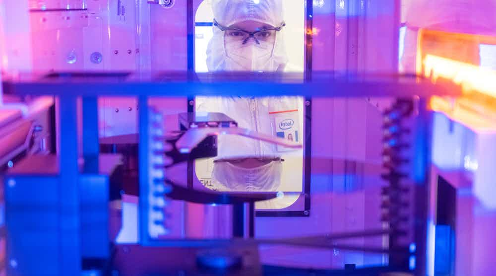
Intelhas officially opened a $3 billion expansion at its advanced technology fab in Oregon, a move the chip giant hopes will help it regain the crown in semiconductor process technology.
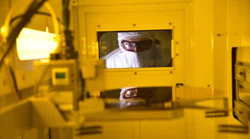
The chip-making giant said the site, known as D1X, serves as the heart of its research and development operations, where it crafts each new generation of logic chips. Intel said the new phase of construction, called Mod3, expands the larger site’s cleanroom capacity by 20%, giving the company’s engineers an additional 270,000 square feet of space to work on several different process technologies in parallel.
At D1X, Intel develops and tests its latest technology nodes before replicating them at production plants around the world, giving it a major role to play in Intel’s plan to turn itself around after years of struggles.
The site is the headquarters of Intel’s Technology Development unit, which stands on the front lines of advancing Moore’s Law, crafting new transistor architectures, wafer processes, and packaging designs that underpin Intel's processor roadmap. The unit has approximately 10,000 employees, primarily based in Hillsboro, Oregon, and it has a reputation as one of the world’s preeminent process engineering teams.
The D1X plant is credited with innovations including high-k metal gate technology, tri-gate 3D transistors, and strained silicon, which Intel said have all been fundamental to its ability to keep up with Moore's Law.
Manufacturing Revival
The investment in D1X is another prong in Intel’s plan to revive its stalled manufacturing operations.
Intel has fallen behind TSMC in its ability to make the most advanced logic chips in recent years. That has caused it to cede market share toAMD,NVIDIA, and other rivals relying on TSMC and other foundries.
When Pat Gelsinger became Intel CEO last year, he pledged to fix the company's problems and reignite its chip development process. Last year, the company revealed one of its most ambitious roadmaps in years, arguing that it would close the performance gap with rivals with its “20A” node due out in 2024. The “A” stands for angstrom, replacing the “nm” or “nanometer” naming used by semiconductor firms for years.
Chip-making is one of the most complex manufacturing processes in the world. Upgrading a production process to a more advanced node usually takes 18 to 24 months—and often a lot longer than that.
Instead, Intel plans to debut a new node every year through 2025, when it aims to recapture its crown in process technology from TSMC and other rivals with its “18A” node (along with new advanced packaging approaches).
英特尔表示,它正考虑引入股票eral key hardware innovations across the board in the 20A node, including its new “RibbonFET” gate–all–around transistors and “PowerVia” backside power delivery system.
Intel is also expanding the use of EUV—or extreme-ultraviolet lithography—tools, which use ultra-short wavelengths of light to scorch smaller transistors on slabs of silicon. These tools work in a way that reduces the risk of imperfections that can ruin chips, thus increasing yields.
But it also plans to get ahead of rivals with a more advanced technology from ASML called high numerical-aperture (High-NA) EUV, which uses more concentrated beams of light to sear smaller transistors on chips.
Contingency Plans
To regain its leadership on the process technology front, Intel is taking steps to make sure it does not repeat the mistakes that dragged out the development of its 10-nm and 7-nm nodes for years.
Intel blamed the prolonged delays in large part on the company’s overly aggressive strategy for increasing transistor density and the mistake of trying to bundle too many improvements in a single process node.
But Intel is prepared to put its problems behind it, executives have said. While it is still taking risks with new technologies, it has contingency plans in place at every step as it moves to new technology nodes.
It is also working in a more modular way to reduce risk. Intel said that it has uncoupled improvements so that it can shelve or swap out technologies that are giving it trouble or require more time to develop. Intel has apparently started testing PowerVia on wafers with FinFETs instead of RibbonFETs to make sure the backside power delivery scheme is ready before it begins production in the 20A node in 2024.
Intel said it has learned its lesson from its manufacturing struggles: According to Intel, the 18A node, which was expected to be operational by early 2025, is on track for mass production half a year ahead of schedule—in the second half of 2024.
“Since its founding, Intel has been devoted to relentlessly advancing Moore’s Law," Gelsinger said in a statement. "The new factory space will bolster our ability to deliver the accelerated process roadmap required to support our IDM 2.0 strategy."
Rebuilding its technology development is only part of his plan to reinvigorate Intel. The company is also expanding and upgrading its production plants to cater to clients of its up-and-coming foundry business.
Intel has pledged a huge amount of spending over the last year to expand its production output at sites in the U.S., Europe, and other regions. At the start of the year, Intel said it would spend at least $20 billion to build its new factories outside of Columbus, Ohio, complementing its vast operations both in Oregon, where the D1X plant is located, and Arizona, where it is also investing $20 billion in two new facilities.
Intel has signed mobile chip giantQualcommas a foundry customer for chips based on its 20A node.
Rebuilding U.S. Fabs
Intel said that the D1X investment reinforces its commitment to U.S. leadership in semiconductor R&D.
Intel’s operations in Oregon are its largest concentration of facilities and talent in the world, with almost 22,000 employees. The expansion brings Intel’s total investment in the state to approximately $52 billion.
“These groundbreaking process innovations all originated right here,” said Ann Kelleher, head of Technology Development at Intel. “Semiconductors are fundamental to U.S. technology leadership, our economy, and supply chain resilience."
It is also renaming the site to Gordon Moore Park site to honor Intel’s co-founder and to remind the world that Moore’s Law, which holds that the density of transistors doubles about every 2 years, is not dead yet.
Gelsinger was joined at the opening ceremony for the D1X expansion on Monday by Oregon Governor Kate Brown, U.S. Senators Jeff Merkley and Ron Wyden, and U.S. Representative Suzanne Bonamici.
As it looks to become an even more sprawling behemoth that builds chips for both itself and others, Intel hopes to win some of more than $50 billion in subsidies from the U.S. government to build chip fabs.
