What you'll learn:
- 应用CTSD技术信号链的设计。
- Advantages of CTSD converters over discrete-time ADCs.
The CTSD topology offers possibilities for optimizing signal chains beyond traditional architectures. Many of today’s applications require smaller form factors but still demand the same performance. Developers are often faced with the question of how to realize this and frequently make do with compromises.
For example, it’s possible to reduce the form factor by sacrificing noise performance or accuracy. This article explores using a continuous-time sigma-delta (CTSD) converter as a new way to optimize the design and reduce bill of materials (BOM) costs and form factor.
Optimizing the Design
To achieve an optimal yield of the desired sensor or signal, all elements in the signal chain must be perfectly coordinated. Several discrete components are usually used, from the sensor to the analog-to-digital converter (ADC). Apart from the sensor and the ADC, oftentimes there are instrumentation amplifiers, ADC drivers, reference buffers, and filters. The selection of an appropriate ADC driver and the filter design, in particular, represent sources of error that are repeatedly underestimated.
One way to optimize the design and reduce BOM costs as well as form factor is to use μModule devices. These devices are highly integrated solutions containing the converter as well as buffers and passive components. With this new CTSD technology, it’s possible to drive the ADC directly without having to use an amplifier as a buffer. In addition, the new topology allows for simplification of the filter design.
DT-ADCs vs. CTSD Converters
Figure 1shows the difference between the traditional discrete-time ADCs (DT-ADCs) and CTSD converters. Compared with the traditional design, the CTSD design allows for a reduction in form factor of up to 68%.
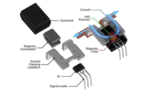
Traditional DT-ADCs, such as SAR ADCs or sigma-delta ADCs, use the switched capacitor topology is used. This is found on the ADC and reference inputs. Differentiation is made between the two phases “sample” and “hold.” They correspond to charging and discharging of the “hold” capacitor. Hence, there must be enough current supplied for charging and discharging as well as charge absorption due to parasitic properties (charge injection kickback)(Fig. 2).
Many sensors are unable to supply such high currents and hence require buffering. Apart from this function, the driver must be fast enough (short settling time, high slew rate) for the output at the end of the “sample” phase(Fig. 2c)解决,没有额外的错误是introduced into the desired signal. Thus, the demands placed on the ADC driver are very high.
A CTSD converter has a resistive input and can be driven directly by the sensor. If the sensor can’t drive the ADC (for example, if the sensor has a very high impedance), a simple amplifier can be interposed for impedance transformation.
A further advantage of the CTSD is the inherent antialiasing filter (low-pass filter) property. With traditional topologies, low-pass filters are needed at the inputs to filter unwanted high-frequency signals.
The reason for this is the Nyquist criterion, which states that the sampling rate must be at least twice as high as the frequency of the desired signal. If the sampling rate is too low, aliasing may occur and undesired noise may fold over into the signal. One explanation for the inherent antialiasing filter properties of CTSD converters is that the sampling doesn’t occur right at the modulator input, but rather after theloop filter.
Conclusion
The CTSD topology offers a further, new possibility besides the traditional architectures for optimizing signal chains. If the time to market, BOM, or form factor plays an important role as well, ADCs such as theAD4134represent good alternatives. Thanks to their resistive inputs and inherent filter properties, numerous designs can be simplified and optimized with them. In many applications, ADC drivers, passive components for the filter design, and reference buffers can be eliminated.