This article is part of theTechXchange:Delving into EMI, EMC and Noise
This article appeared inMicrowaves & RFand has been published here with permission.
What you’ll learn:
- What are the drivers of conducted and radiated emissions?
- Different methods for reducing FM band conducted EMI, which are simple to implement and low cost.
Although EMI shields and ferrite clips are often a sought-after EMI solution, they can be expensive, bulky, and sometimes insufficient. FM band EMI noise can be reduced by understanding where it’s coming from and employing circuit and PCB design techniques to suppress it at the source.
EMI性能供电网络的评论家al in noise-sensitive systems such as automotive circuits, especially when switch-mode power supplies (SMPS) are involved. Engineers can invest significant time to reduce conducted emissions (CE) and radiated emissions (RE). In particular, when measuring CE, the FM band (76 to ~108 MHz) can be the most difficult region to achieve a passing result. Designers might need to spend significant time to do so. Why is the CE noise in the FM band so difficult to mitigate?
Low-frequency (AM band) CE is dominated by differential-mode (DM) noise. High-frequency (FM band) CE is dominated by common-mode (CM) noise.1Common-mode noise current is generated by nodes with changing voltages on the PCB. The current leaks through stray capacitance to reference ground and back to input plus and minus cables(Fig. 1). Due to the complexity of stray capacitance around the PCB, it’s not practical to simulate stray capacitance and estimate FM band conducted EMI. Rather, it’s best to test the board in an EMI chamber.
There are proven methods in the lab that effectively reduce FM band EMI, including changing switching frequency, switching slew rate, switch node layout, hot-loop layout, inductors, and even the location of input cables and load. The efficacy of each method could vary from board to board.
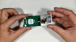
This article examines a number of simple, low-cost ways to reduce FM band conducted EMI on a board—without using ferrite clips or shields. The results are verified by performing current-probe CE tests, in a certified EMI chamber, on a board featuring theLT3922-1in an automotive HUD LED driver(Fig. 2).
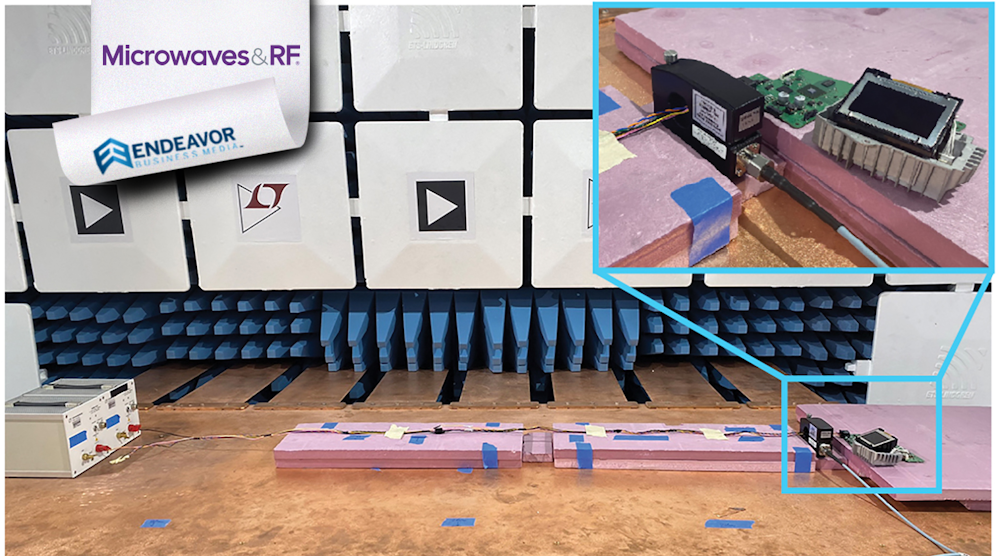
In this test, CE is measured with a current-probe method in a CISPR 25 EMI setup(Fig. 3). CE can be tested by either the voltage-probe method or current-probe method, but the current-probe method standard is generally considered the stricter of the two.
Instead of measuring the voltage output from the line-impedance stabilization networks (LISNs), the current CE method utilizes a high-bandwidth current probe to measure CM noise signals propagating through the power cord or harness, at distances of 50 mm and 750 mm from the DUT. Peak and average CE data is collected at each sweep and compared against published standards limits.
For the current-probe method, FM band average CE limits described in CISPR 25 Class 5 are as low as −16 dBµA. Here, we present several effective approaches to improving results in the FM band under current probe testing for CE. Many of these methods can be applied to improve results in voltage method CE testing as well.
All of the tests in this study feature spread-spectrum frequency modulation (SSFM) enabled, unless otherwise specified. SSFM reduces EMI spikes at the switching frequency as well as its harmonics.
共模扼流圈抑制EMI噪声调频乐队
CM noise current, which is generated during switching, leaks into the reference ground through stray capacitance and comes back through input supply and return paths in the same direction. By increasing the common-mode impedance in the loop with a CM choke, unwanted CM noise can be suppressed.
Figure 4shows 50- and 750-mm average current-probe CE results, comparing the original circuit without the choke and with the choke installed before the LED driver circuit. The ambient noise floor is also shown for reference. FM band CE (76 to ~108 MHz) was reduced by more than 8 dBµA.
Inductors Make a Difference
适用于快速变化的电压和电流the main inductor, making it an electromagnetic antenna. Therefore, inductors could be a source for the FM band CE noise. EMI test results can be improved through a number of inductor-related methods. For instance, the assembly orientation of the inductor can make a difference.2
Shielded inductors usually have lower emissions than unshielded ones, and some core materials limit H-field and E-field radiation more than others. For example, iron powder and metal alloy powder inductors have less E-field shielding effectiveness at frequencies above 1 MHz. MnZn and NiZn perform better at higher switching frequencies.2,3Inductors with exposed pads perform worse than hidden pad inductors. Connecting the long lead of the inner coil winding to the high dV⁄dt (switch) node can increase E-field radiation dramatically.
Three 22-µH shielded inductors were tested(see table). EMI was evaluated in the same circuit without a CM choke, and each inductor was assembled in its best performing orientation. The results are compared inFigure 5. In this study, the Coilcraft XEL inductor yields the best FM band performance, reducing FM band EMI by 5.1 dB compared to a 3L inductor.
Lower Switching Frequency Results in a Quieter FM Band
Reducing the switching frequency (fSW) lowers the emissions energy at a given high frequency. InFigure 6, current probe CE is tested without a CM choke and compared at 200-, 300-, and 400-kHz switching frequencies. All of the components other than RT were kept the same. The 200-kHz test shows the lowest EMI in the FM band, with emissions 3.2 dB lower than the 400-kHz case.
Shrink Your Noise Antenna by Reducing Switch-Node Area
The high dV⁄dt switching node is a noise source that generates capacitive coupling and increases CM EMI noise in CE. It also works as an antenna, which radiates electromagnetic noise into the space, affecting radiated EMI as well. Therefore, a minimized switching-node area on the PCB layout improves EMI performance.
To test this on a PCB board, the switching node area was reduced by cutting off some copper and moving the inductor closer to the IC(Fig. 7). EMI was tested before and after the copper removal(Fig. 8).
The 50-mm current-probe CE test decreases 1 dB at 105 MHz, while the 750-mm test doesn’t show obvious improvement. This result indicates the copper area isn’t the main contributing factor to FM band EMI for this application. Still, it’s worth trying to reduce switch-node area as much as possible to achieve a low-EMI PCB layout, or during EMI mitigation.
Conclusion
A power supply’s EMI performance depends foremost on the performance of the power-supply IC, but even a high-performance IC can only deliver low EMI with proper selection of components and effective PCB layout. In this article, we explored several methods of mitigating conducted emissions in the FM band.
Applying a CM choke on positive and negative input lines increases impedance in the common-mode noise current loop. Different inductors with different core materials, core constructions, and coil constructions yield a range of EMI performance results. It’s difficult to estimate which inductor is best by looking exclusively at specs, but comparisons can be made in the EMI lab. The assembly orientation of inductors on the PCB is also important.
Reducing switching frequency and reducing switching-node copper area can both help lower FM band CE. If the DUT is a switching-regulator circuit using a controller part (external MOSFETs), FM band EMI can be further shrunk by reducing switching slew rates and minimizing hot loop areas.
Read more articles like this at theTechXchange:Delving into EMI, EMC and Noise
References
1. Ling Jiang, Frank Wang, Keith Szolusha, and Kurk Mathews. “A Practical Method for Separating Common-Mode and Differential-Mode Emissions in ConductedEmissions Testing.”Analog Dialogue, Vol. 55, No. 1, January 2021.
2. Szolusha, Keith and Li, Gengyao. “Does the Assembly Orientation of an SMPS Inductor Affect Emissions?”emiTime, August 2020.
3. Bramanpalli, Ranjith. “ANP047: The Behavior of Electro-Magnetic Radiation ofPower Inductors in Power Management.” Würth Elektronik, March 2018.

