
|
|
以.pdf格式下载本文 此文件类型在适用时包括高分辨率图形和原理图。 |
Modern telecommunications applications like 4G Long Term Evolution (LTE) systems as well as forthcoming 5G systems use multicarrier modulation like orthogonal frequency-division multiplexing (OFDM) with quadrature amplitude modulation (QAM). To meet user demands for ever-higher data rates, the system must have wide bandwidth and be able to process both high- and low-amplitude signals.
由于大多数信号处理都是数字处理,因此必须在某个时候将传入信号转换为数字。一种解决方案将是具有高动态范围和在千兆位范围内采样率的宽带宽度类似物到数字转换器(ADC)。现在可以使用这样的ADC。
Receiver Architectures
接收器体系结构的三种基本形式用于电信和其他软件定义的Radio(SDR)应用程序:SuperHeterodyne,Direct Conversion和RF采样(见图)。The superhet form(见图,A)是传统的,仍然广泛使用。它采用传入的RF信号,并用混合器将其降低到较低的中间频率(如果)。保留信号调制和带宽,但采样率要求要低得多。
The superhet has some downsides, though. First, it requires many circuits and filters, which bumps up the cost. Also, the local oscillator (LO), usually a PLL synthesizer, adds phase noise and jitter. On top of that, the mixing process makes the receiver subject to images depending on the frequency bands being used. A dual-conversion architecture with a second mixer and LO solves this problem, but adds more cost and complexity.
更简单的安排是直接转换接收器(见图,b)。LO频率等于传入的信号频率,导致差为零。如果接收器为零,则此体系结构将RF信号直接转换为基带。需要更少的电路和过滤器,从而降低成本和复杂性。放松的ADC采样率是有益的,并且消除了超级现象的图像问题。另一方面,直接转换接收器遭受直流偏移问题的损失,并泄漏到输入。
An ideal receiver architecture employs direct RF sampling, where the incoming signal is sent straight to the ADC for conversion. This hasn’t been possible until recently, as ADC sampling rates have increased to accommodate the higher RF frequencies including microwave spectrum. In the basic arrangement(see figure, c),一些前端过滤缩小了感兴趣的乐队的覆盖范围。ADC将整个输入转换为随后通过DSP方法处理的数字位流。直接RF采样大大简化了设计并最小化成本和复杂性。但是,它需要快速的DSP或FPGA才能跟上数字化率。幸运的是,快速ADC和处理芯片现在可以实现此类接收器。
ADC考虑
采样ADC的关键规范是,采样率必须至少是两倍bandwidth信号正在数字化。没错,带宽或更多。据称,更多的是过采样,有助于保留被数字化的信号的细节。过采样还减少了量化噪声,从而提高了信号噪声比率(SNR)。
For example, assume that you need to digitize a group of LTE carriers, each typically 20 MHz wide. The most common scenario is a group of multiple 20-MHz carriers. Sometimes large spaces exist between groups of carriers.
考虑四组十个20 MHz携带者,每个载体彼此之间的间隔65 MHz。那是800 MHz的载体,3×65 = 195 MHz的间距,总带宽为995 MHz。在2 GHz范围内的一些分配的蜂窝频谱频率周围,该带宽最多可达1 GHz的带宽。您将需要最低样品率为2 GB/s的ADC。但是,3或4 GB/S会更好。
One key point to consider: The ADC is going to convert everything within the input bandwidth. Only one ADC is needed, and it doesn’t care if there are gaps in the digitized spectrum. The big problem now isn’t the sampling rate, but how fast the processing can be done. It will take lots of DSP filtering to sort out the individual 20-MHz channels, as well as perform demodulation and other functions. That calls for fast FPGAs or DSPs and a high-speed interface from ADC to FPGA or DSP.
One solution to the processing-speed problem is to take the ADC output and subject it to the process of decimation. Decimation is the process of removing samples from the ADC output at regular intervals, thereby decreasing the sample rate to a range that can be managed by the processing circuits. Decimation is usually carried out by a FIR filter and an anti-aliasing circuit. The sampling rate can also be reduced via digital downconversion with a digital mixer, numerical-controlled oscillator (NCO), and DSP low-pass filter.
快速ADC的示例
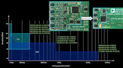
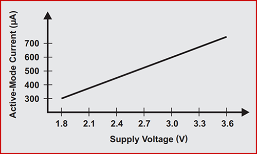
Texas Instruments的ADC32RF45是可以实施直接RF采样接收器的ADC。它提供了充满挑战的无线应用所需的宽带宽度和高动态范围。ADC32RF45,双通道,14位,3个样本/S ADC,保持模拟输入带宽为3.2 GHz。一些典型的规格包括69 dB的虚假动态范围(SFDR),SNR为62.7 dB和–155 dbfs/hz的噪声底。
一个重要的功能是在每个ADC渠道之后包含具有多达三个独立NCO的数字下调器。该界面是与DSP,FPGA和ASIC相连的JESD204B。每个ADC有四个车道,速度高达12.5 GB/s。
Besides its use in direct RF conversion receivers for cellular, the ADC32RF45 will find applications in MIMO arrays, beamforming, phased-array radar, electronic-warfare equipment, microwave backhaul, cable and wireless broadband, test instruments, and other SDR designs. TI offers the ADC32RF80EVM evaluation module to get you up to speed quickly in designing.
TI offers a series of instructional videos that further elaborate on the ADC32RF45 and its capabilities and uses: