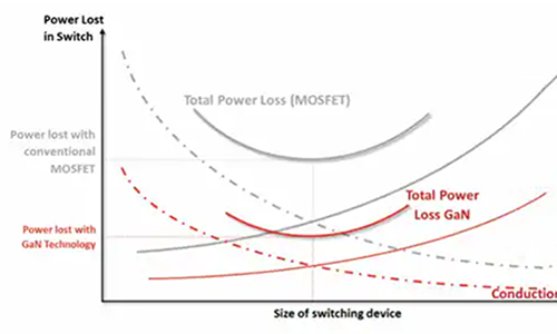
Wide-bandgap (WBG) power electronics devices reduce component size, increase efficiency, and improve performance for hybrid and all-electric vehicles. In particular, gallium nitride’s (GaN) exceptionally high electron mobility and low temperature coefficient allows for very low on-resistance (RDS(on)), while its lateral device structure and majority carrier diode provide low total gate charge (QG) and zero reverse-recovery charge (QRR).
The end result is a device that can handle tasks where very high switching frequency—which translates into lower switching losses and lower drive power—and low on-time are beneficial. It also improves results where on-state losses might otherwise dominate.
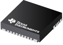
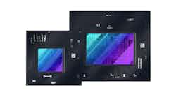
Mini GaN Transistor
As an example,Efficient Power Conversion(EPC) announced the production release of theEPC2050, a 350-V GaN transistor with a maximum RDS(on)of 80 mΩ and a 26-A pulsed output current. The EPC2050 measures just 1.95 × 1.95 mm. According to the company, the tiny size enables power solutions that occupy 10X less area than comparable silicon solutions. Automotive applications benefiting from the fast-switching speed and minuscule size of the EPC2050 include fast chargers, battery-management systems, LiDAR, and LED lighting.
“With the EPC2050, designers no longer have to choose between size and performance—they can have both and lower cost!” says Alex Lidow, EPC’s CEO.
EPC’s GaN FETs behave similarly to silicon power MOSFETs. A positive bias on the gate relative to the source causes a field effect. This attracts electrons that complete a bidirectional channel between the drain and the source. When the bias is removed from the gate, the electrons under it are dispersed into the GaN, recreating the depletion region and once again giving it the capability to block voltage.
The relatively high frequency response of GaN FETs is an improvement over prior silicon devices and an added consideration for the user when laying out circuits. Still, EPC says users can leverage their past design experience and achieve new levels of performance in their products.
EPC also notes that its GaN transistor structure is a purely lateral device, absent of the parasitic bipolar transistor common to silicon-based MOSFETs. As such, reverse bias or “diode” operation has a different mechanism but similar function. With zero bias gate to source, there’s an absence of electrons under the gate region.
As the drain voltage is decreased, a positive bias on the gate is created relative to the drift region, injecting electrons under the gate. Once the gate threshold is reached, there will be sufficient electrons under the gate to form a conductive channel. The benefit to this mechanism is that there are no minority carriers involved in conduction, and therefore no QRR.
Dev Board Details
EPC’sEPC90121development board is a 350-V maximum device-voltage, 4-A maximum output-current half-bridge featuring the EPC2050, and onsemi’s NCP51820 gate driver. The board measures 2 × 2 in. and contains all critical components; the layout supports optimal switching performance. In addition, various probe points facilitate simple waveform measurement and efficiency calculation.
The purpose of this development board is to simplify the evaluation process of the EPC2050. It includes all of the critical components on a single board that can be easily connected into many existing converter topologies.
EPC t进行了广泛的可靠性测试o continue to better understand the behavior of GaN devices over a wide range of stress conditions. At EPC, GaN devices have been in volume production since March 2010 and the company claims it has demonstrated high reliability in both laboratory testing and high-volume customer applications.
What’s more, EPC says the results of these reliability studies show that GaN is an extremely robust technology, and it continues to improve at a rapid pace. The company is committed to subjecting GaN devices to rigid reliability standards and sharing the results with the power-conversion industry.
EPC2050 GaN FETs are supplied only in passivated die form with solder bumps. They’re priced at $3.05 each in 1,000 units. The EPC90121 development board costs $156.25.


_pushing_performance_beyond_silicon.png?auto=format,compress&fit=crop&h=139&w=250&q=1)