
What you'll learn:
- NAND FLASH LEVEL类型的比较。
- 伪SLC与TLC和其他人有什么好处?
- How pSLC creates new storage capacities.
Today's NAND flash technology industry is awash with success stories about reaching new memory densities. The technology has long since achieved well over 100 layers, and there seems to be no limit anytime soon.
The steady increase in the number of layers goes hand in hand with the trend to store more bits per cell. The current mainstream technology is triple-level cell (TLC). It stores three bits per cell, where the term “level” refers to the number of bits, not the internal states. The number of internal states that need to be safely stored and read again are to the power of two of the number of bits stored, meaning that with three bits, eight different states need to be recognized. The trend is toward even more memory for the same chip size, which is realized by quad-level cell (QLC), four bits per cell, which has the demanding task of managing 16 states.
The increasing amount of stored information per square centimeter of silicon will decrease the number of feasible write cycles. While with single-level cell (SLC), one bit per cell, it was still possible to rewrite each cell 60,000 to 100,000 times, with multi-level cell (MLC), two bits per cell, the number was reduced to 3,000.
在从平面MLC到3D TLC的过渡中(两个与三个位),由于具有3D电荷陷阱闪光灯的较好的单元格性,因此可以维持3,000周期的寿命。在QLC的情况下,该值降低到约1,000个,下一个进化阶段的值小于100:PENTA级单元格(PLC),每个单元格五位= 32个状态。
PLC不再处于原型阶段。随着时间的流逝,它将成为超级数据中心应用程序的主流NAND,例如Google或Facebook的应用程序,其中只有一次数据写入一次并经常读取 - 读取一次,请阅读多个(WORM)。
High Demands Have Their Price
相比之下,仍然存在编写大量小数据的应用程序,无论是传感器数据的记录,本地物联网数据库还是状态信息的记录。在字节到千字节范围内编写小包装量的速度比Megabyte系列中的数据传输速度要快得多。
对于这些应用,SLC以前是最好的存储介质。由于小块尺寸和最多100,000个可能的擦除周期,因此基于SLC的存储模块通常比现场所需的运营生活更耐用。此外,SLC的温度敏感性较低,并且对控制器的误差校正要求较低,所有这些要求对长期性能产生积极影响。
但是,在这些苛刻的应用中替换SLC的主要原因归结为另一种重要的考虑因素。SLC技术遇到了“鸡肉和蛋”的困境:由于较旧,更昂贵的技术,主流逐渐脱离SLC,这就是为什么不值得将SLC转移到更现代的技术的原因。
Pseudo-SLC as an Attractive Middle Ground
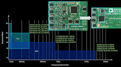
Today's SLC technology has a maximum capacity per chip of 32 Gb with a typical chip area of 100 mm². A common and similarly priced 3D NAND TLC chip, on the other hand, has 512-Gb capacity and in the next generation will reach 1 Tb. It makes TLC technology 16 times less expensive than SLC.
This effect is put into perspective at the system level: TLC controllers are more complex and more expensive, and with 512-Gb NAND chips, the minimum capacity of a drive is equal to 32 GB. This isn’t a problem for data centers or ambitious home users. In these scenarios, interesting drive sizes tend to start beyond 1 TB anyway. However, the situation is different for applications in the industrial sector or as a boot drive for network or communication systems. In these cases, a few gigabytes, albeit used more intensively, is usually sufficient.
Since only one chip is used in the 32-GB TLC case described above, the drive offers a rather low write and read speed, regardless of its interface, because the system performance results from the number of parallel flash channels—the more channels that are equipped, the higher the performance. High-speed SSDs use up to 16 parallel flash channels to achieve the corresponding performance. With several parallel SLC flash chips, a fast SSD also can be realized with much smaller capacities.
理想的是具有大量生产的现代3D NAND技术的SLC芯片,因此具有成本效益。记住SLC的定义(即每个单元格),所有现代NAND Flash产品的确是可行的。但是,必须告知内部控制器仅与两个州一起工作:删除和编程;1或0。这种操作方式称为PSLC或伪SLC。
优势超过了缺点
By using only two internal states, programming can be achieved with a lower voltage. This protects the sensitive silicon oxide in the memory transistor and extends its life. Since the electronics must only distinguish between two states, the signal-to-noise ratio is much greater than in cases where 32 states are present. Degradation of the stored value can be tolerated much longer than with TLC or QLC.
Both effects mean that the permitted number of programming or erasing cycles increases from 3,000 for TLC to a figure between 30,000 and 60,000 for pSLC. It brings this operating mode back into the range of “real” SLC technology.
二维多层陶瓷NAND在pSLC也能够操作mode. Here, only one of the two bits per cell was used, thus halving the capacity. Writing only one bit also delivered speed advantages. Costs per bit doubled, of course, since only half the bit capacity was available per silicon chip.
With TLC technology, only one of three bits per cell is used. Therefore, the cost triples to achieve the same storage capacity. Nonetheless, this is still much cheaper than with real SLC NAND.
另一方面,在PSLC模式下使用QLC没有任何优势。QLC的能力为1.33倍,但您只使用每个单元格的四分之一。结果,QLC和TLC的PSLC容量相同。
pSLC Leads to “New” Storage Capacities
Reducing the chip capacity to one third has an unusual effect on the commonly used SSD capacities. In the binary IT world, people were accustomed to calculating with multiples of two: 64, 128, 256, 512, etc., GB drive capacity.
However, with the transition to 3D NAND, more memory was needed internally to realize caches or RAID, or so-called overprovisioning, where extra reserved memory is used to speed up writes and increase lifetime. The resulting capacities are then 30, 60, 120, 240, 480, etc., GB.
用户可用的容量由参数“用户LBA范围”表示。经常在声称“二进制尺寸”的SSD的规格中看到,其中“用户LBA范围”实际上已缩短到了这一程度。在这种情况下,驱动器显示512 GB,但用户只有480 GB可用。在这里提出谨慎的态度,因为具有此细节级别的制造商规格非常罕见,因此实际容量通常仅在操作过程中发现。
如果现在添加了PSLC减少,则会导致不同寻常的新驱动器尺寸:480-GB TLC SSD变为160 GB PSLC SSD,其昂贵,就像480-GB TLC SSD一样昂贵。使用固定的系统环境图像的嵌入式或网络和通信扇区的客户仍然使用二进制尺寸来实现小容量。对于这些情况,然后将用户容量降低到下一个较小的二进制容量,其优势是,服务寿命再次较大。但是,可用容量的每千兆字节的价格也略有上涨。
Conclusion
pSLC optimally complements classic SLC memory technology and is an ideal solution for cost-effectively adapting 3D NAND technology to the lifetime of SLC. The only disadvantage is the unfamiliar new drive sizes like 10, 20, 40, 80, and 160 GB.
因此,工业记忆制造商Swissbit还提供pSLC模式几乎所有的选项products with MLC and 3D TLC NAND. True SLC products will remain in the company’s range in the long term because the advantage of true SLC is the fact that it no longer needs changing every two years, thereby saving the costs of requalification. For markets like medical technology, automation, or transportation with very long product life cycles and onerous standardization requirements, there’s still no alternative to real SLC. That’s why it’s important to have a reliable memory partner with long-term customer solutions.