Off-chip storage is critical to many micro and system-on-chip (SoC) applications. High-end applications can justify interfaces like DDR3 and DDR4 and even larger flash storage can be accessed using SATA and PCI Express. Unfortunately this is often overkill for many applications where the pin count, speed, or power requirements for these are too high. Likewise, at the low end, interfaces such as SPI, quad SPI (QSPI), and I2C are too slow.
This middle ground is whereSpansion’sHyperBus comes into play (see “How HyperBus Delivers 330 Mbyte/s Using a Dozen Signals”). It can deliver 333 Mbytes/s of bandwidth that is more than five times faster than QSPI. It uses 12 signals of which 8 are data signals (Fig. 1). The other signals include a differential clock, chip select, and read data strobe.
HyperBus operates at 1.8 V and 3 V. The latter runs with a 100 MHz clock and uses only 11 lines since it does not use a differential clock. The 1.8 V version uses CK and CK# signals that run at 166 MHz. It uses a double data rate (DDR) transfer mode, hence the 333 MHz bandwidth.
The HyperBus operates like many serial memories. Each transaction begins with a 6-byte command/address sequence. Three bits of the first byte are used for the commands that include read, write, and burst mode. This leaves 45 bits for addressing, although a few more bits may be reserved for future use. That would still leave a 40-bit address space.
The write transaction for the 1.8 V writes 2 bytes of data. The read data strobe (RDS) is not used for write transactions. The delay until the next transaction is usually enough for a flash device to store the data. Multiple writes are handled via multiple transactions.
|
|
Download this article in .PDF format This file type includes high resolution graphics and schematics when applicable. |
Spansion HyperFlash is a NOR flash device that supports HyperBus. It supports a wrapped burst mode of 16, 32, and 64 bytes. Multiple HyperBus devices can operate using the same data and control lines, but each requires its own chip select line. In theory, it would be possible to use reserved bits for addressing, but that is not something the current crop of devices will support. In practice, a single device will be the normal configuration unless a HyperFlash RAM is required.
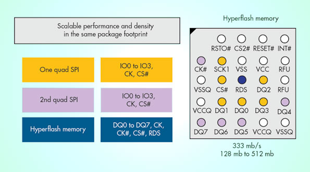
The initial memory device available with a HyperBus interface is some NOR flash memory (see “HyperBus Accelerates NOR Flash Storage”). These devices are available in 8 mm by 6 mm packages (Fig. 2) with capacities up to 512 Mbits. The pinouts on the chip are designed to handle HyperBus as well as dual QSPI interfaces (Fig. 3). This provides an upgrade path for designs that initially support QSPI.
HyperBus memory devices are not too useful unless there is a processor that can take advantage of the storage. Spansion’s latest Traveo microcontroller (Fig. 4) has an ARM Cortex-R5F core that supports HyperBus (see “微观目标远程信息处理3 d和HyperBus增刊ort”). It also supports interfaces such as CAN and Ethernet AVB.
Traveo目标中档电信applications that are cost-sensitive. Its 2D/3D graphics engine can generate images on the fly. Low-end applications can use on-chip memory. It has 2 Mbytes of flash and 256 Kbytes of RAM. Higher-end applications can utilize HyperBus flash and RAM chips to provide additional features.
HyperBus can work well for other applications like high-resolution digital cameras. The higher bandwidth allows it to handle image capture while keeping costs low.
Spansion’s Hyperbus technology fills a niche. It can provide faster boot times as well as supporting direct execution from off-chip flash that is significantly faster than QSPI. It also provides access to off-chip RAM or flash memory.


