>> Electronic Design Resources
.. >> Library: Article Series
.. .. >> Series: Path to Systems
System-in-package (SiP) technology is at the beginning of its revolution. Some see the SiP in the same way as a system on chip (SoC)—as an IC component with no simple path to further customization. Also, the economics of scale relegate the device to a high-volume manufacturing process in addition to the long design cycle time. Which isn’t an issue if you, as a systems engineer, need millions of devices per year. However, new innovators and entrepreneurs are left out.
So, is there a way that systems designers can take advantage of theSiP technologyto further integrate without the need for a high-volume application? Apparently so, as capabilities loom on the horizon that allow for more integration with less volume using SiP.
SiP Design and Manufacture Today
There are compelling reasons for a SiP to be the solution to systems integration. We detailed several, including simplification, miniaturization, cost reduction, and reliability inPart 2of this series. In fact, the same requirements that drove the SoC development are likely to drive the SiP roadmap as well. However, SiP capability will be able to bypass many of the limitations presented by SoC without sacrificing much of the system integration achievable through an SoC.
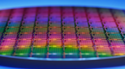
For example,Figure 1shows ablock diagram of a SiP1具有多种功能块。该示例是一个具有不同IP块的嵌入式系统,具有几个不同的半导体过程节点。此外,功能块使SIP集成到系统中。这些子系统中的某些(例如平行和串行接口)集成到SOC中,而其他子系统(例如DDR内存和功率管理IC)是独立的组件集成到SIP中。这使SIP成为功能系统级的块,而不是设计挑战,这已成为当前SOC的情况。
1. OSD335x C-SiP system-in-package block diagram.
图1框图definition is the result of the initial stages of the SiP’s design. An important decision to make here is which components go in the SiP and which do not. Design complexity, functional importance, and package/die size are some of the factors that influence this decision. Once the device is well defined in the block diagram stage, computer-aided design (CAD) tools are used to actualize the SiP device. SiP and IC manufacturers often have specific design rules that may not be common or industry standard. So, it’s important to work with the manufacturer during the design stage. When the design is complete, the release package is sent to the manufacturer.
An example process flow of SiP manufacturing process is shown inFigure 2.理想情况下,SIP中的所有活性组件均处于模具状态,但它们也可以是包装零件。制造过程可能会根据集成技术和要达到的目标大小/规范而有所不同。图2中描述的过程说明了一个简单的表面安装设备(SMD)连接表面安装组件和电线键合的过程。
2. High-level manufacturing flow of a SiP.
SIP的SMD组件连接到基材上。该基板是一个印刷电路板,该电路板构建了微观级设计规则,可实现微型电路板,紧密的集成以及更好的带宽和功率性能。组装通过回流后,它是预先烘烤的,用于模具附件。模具附件固化后,将模具连接并进行电线粘结。该组件再次被烘烤,并用适合系统的预选模具化合物模制。设置了模具化合物后,包装将通过焊球连接和干烘烤。在该过程中嵌入了几个质量检查点,以启用过程特定的故障检测。
克服当前设计和制造过程的挑战
如第2部分所述,这种新的SIP技术提出了新的挑战。技术是技术性的,例如缺乏灵活性和无法自定义的挑战。其他挑战,例如在IC制造过程中需要大量批量生产的挑战是经济的。尽管希望将更多功能块集成到系统中,但这样做会损害系统的灵活性。功能块的数量越大,SIP的灵活性越少,这意味着较低的体积,特定于应用程序和较高的成本,使集成不可行。
Although not as complex as with an SoC design, making changes to a system component in the SiP still provides a significant hurdle. Moreover, users desire customizability to have better control of their own design as well as make choices of the functionality of the SiP. All of this, while possible, has cost and time burdens associated with it. The good news is, there are solutions that can overcome these challenges with minimum effort spent in time and money.
Semi-Custom SIP Devices
Semiconductor manufacturers have developed many solutions over the years that enable higher integration and better manufacturability for SiPs. Flip-chip, 3D die stacking, and package on package (PoP) are examples, essentially adding the z-axis to the integration environment. The flexibility of bond-wire placement and specialized mechanical tools have played an important part in these solutions.
These solutions, however, are either highly integrated and don’t match a lot of system requirements or remain too risky to be integrated into the production flow to be considered as effective enablersThe only way to maintain the scalability of the manufacturing process while delivering more integration and functionality is through customizability, which is transparent to the manufacturing process. By making it transparent, the advances in manufacturing processes and adapting the SiP design process to lend itself to customization can be an ideal solution.
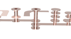
For example,Figure 3显示一个版本a customizable part (connection matrix) of a substrate.2中央垫(25)就是一个死会附加to the substrate and bond wires would be used to connect the die pads to appropriate substrate pads as needed. The central pad can accommodate different-sized dies. This layout can be used to make a configurable SiP by programming the pick-and-place machine and the wire-bonding machine appropriately.
3.可自定义的模具足迹。
这只是一个相当简单的示例,说明了可配置的设计选择如何导致可自定义的SIP。另一个示例,或者是该模具结构配置的扩展,是可配置的基板布局,允许在多个模具之间连接信号。Figure 4显示可自定义的互连矩阵,可用于创建可配置的SIP系统。图3中的模具组件以及其他被动/活动组件的信号可以连接到所示的连接矩阵Figure 4by signal traces on the substrate. Then they’re electrically connected to other signals with bond wires on the connection matrix. In a sense, this makes the connection matrix, when combined with the die-attach pads, a miniature breadboard.
4. Customizable interconnection matrix.
中央连接矩阵和互连矩阵的这种组合具有多种应用。例如,信号调节。具有许多连接矩阵和被动组件的互连矩阵连接到围绕其围绕基质的互连矩阵(图5)can allow for a large number of op-amp-based signal-conditioning systems.
5. Customizable substrate design.
As mentioned, this is one of many ways to create a customizable substrate. The takeaway here is that customizability is a design methodology that increases flexibility and enables low-volume innovators while providing access to the latest and greatest integration methods.
So, the next question is, “How can the design of a SiP be done to build configurable SiPs?” Based on the application, there are many answers to this question. While the above example is suited for signal conditioning, similar design methodology can be implemented for other areas of computing and embedded design.
What Are the Issues?
The configurable SiP creates a new set of challenges. For example, new software tools that enable this design methodology are necessary. Challenges on the manufacturing side include programming the capability in the pick-and-place/bond-wiring machines such that a production line delivers different customizations of a configurable SiP while the line remains the same.
结论
The customizable SiP solution, as it progresses and morphs into new SiP designs, represents a new paradigm in semiconductor manufacturing. The end goal of this technology is to provide a SiP to the system designer who has a need for low-volume run rates with the cost associated with a high-volume run rate.
Is there a system that allows individuals to input their designs while delivering SiP’ed packages without the drawbacks of the low-volume manufacturing cost as well as complex design effort? Such a design methodology reduces time and money spent on the design while providing a path to integration beyond standard components on a PCB. We believe the answer is yes.
- Series: Path to Systems
- 本系列的先前文章...为什么要sip?
- Next article in this Series ... A SiP of Reliable Advantage—Systems Under Test
References:
1.https://octavosystems.com/octavo_products/osd335x-c-sip/
2.https://patents.google.com/patent/wo2017040967a1/en?oq=wo2017040967