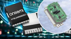
5G system hardware designers are challenged to implement better power solutions that help all necessary electronics to fit into form factors close to those of existing 4G base-station enclosures while maintaining a low EMI.
Increased board component density in 5G systems demands space-saving solutions with higher efficiency and lower EMI than traditional discrete dc-dc ICs with external inductor-based solutions. This will challenge designers to create a careful layout of components for filters to minimize radiated and conducted EMI generated via power converter and inductor switching currents.
It’s no secret that dc-dc converters are notorious for conducted EMI coming from magnetic fields emanating from the current loop path. That path is comprised of the output switching node to ground as well as the input capacitor to ground.


